Insulators
Every high voltage vacuum system contains at least one insulator, and every insulator carries at least two triple junctions: the lines where metal, ceramic, and vacuum meet. Almost everything that goes wrong at high voltage in vacuum begins on one of those lines. The argument for why, and the story of the largest machine ever built to confront it, live in the essay The Third Point. This page is the reference that stands behind it: the family of parts, the physics in brief, the rules the tube houses never wrote down, and the numbers worth carrying in your head.
The point
An insulator in vacuum rarely fails through its body. It fails along its surface, and the surface event starts at a junction. At the line where metal, dielectric, and vacuum meet, the local field can run an order of magnitude above the average; microscopic gaps between metallization and ceramic push it further. At the cathode side junction, that enhancement drives field emission, and emission grows exponentially with local field, which is why small geometric sins cost decades of performance. Emitted electrons strike the ceramic; if each impact frees more than one secondary, the surface charges positive and pulls the next generation back down. The avalanche hops along the surface, desorbs adsorbed gas, and the flashover completes through that gas blanket: a vacuum breakdown that is really a surface-gas breakdown.
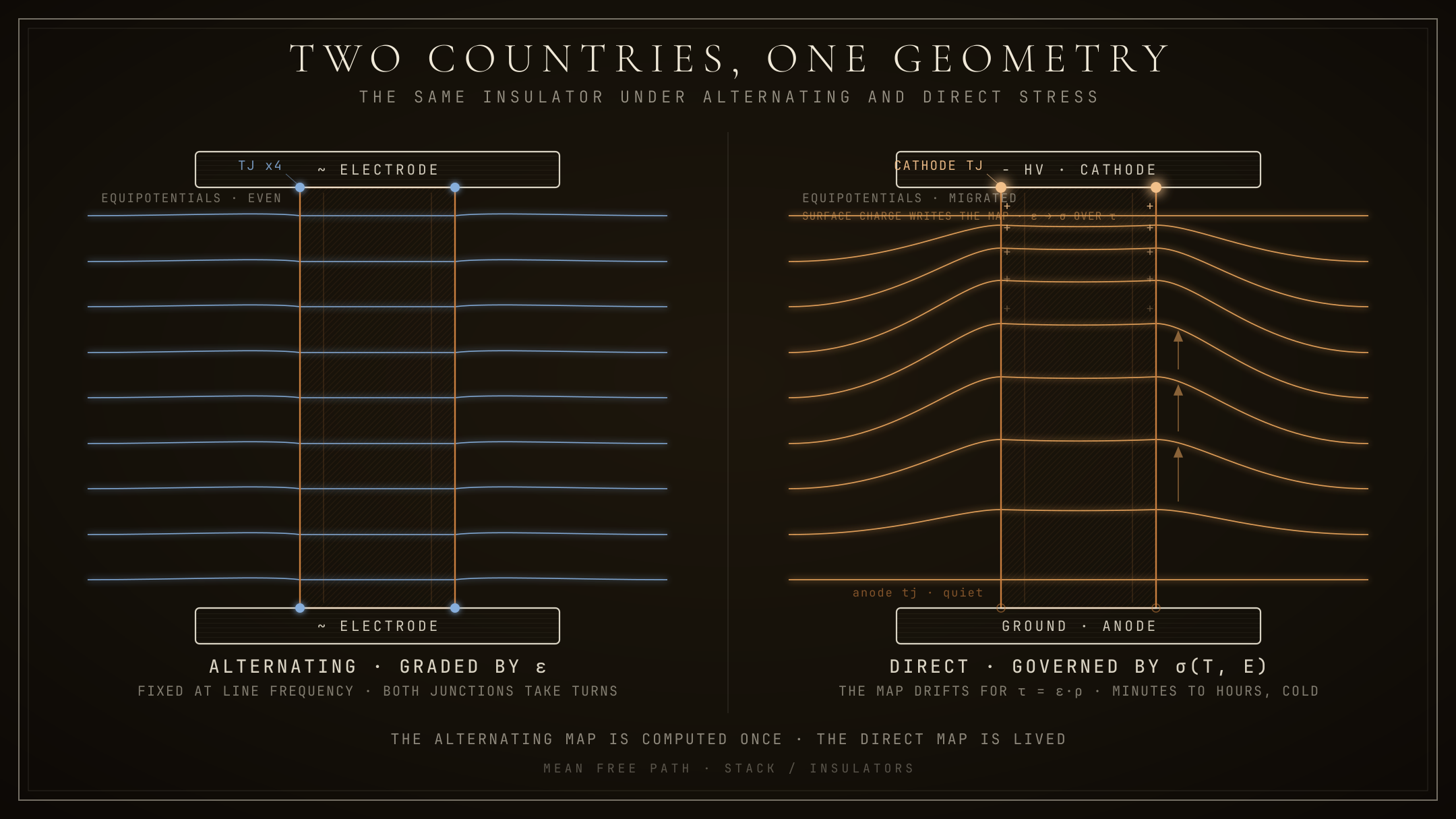
Under alternating stress the field map is set by permittivity, is computed once, and holds; both junctions take turns as cathode, and the design must be symmetric. Under direct stress the map belongs to conductivity, which in alumina varies by orders of magnitude with temperature and field. The DC map settles on the timescale tau equals epsilon times rho, minutes to hours at room temperature, seconds when hot. A DC insulator is therefore a history: charge state, conditioning record, temperature profile. One junction is critical, which is a gift; you can spend your whole budget on it. The full argument is in The Third Point. The rules below are what it buys you.
Six shapes cover most of what industry brazes to a flange. They differ in geometry and in what crosses them: mechanical load, signal, current, potential, or microwave power. They share one anatomy: a ceramic body, a metallized or active-brazed edge, and junctions that set the voltage the whole assembly will actually hold.
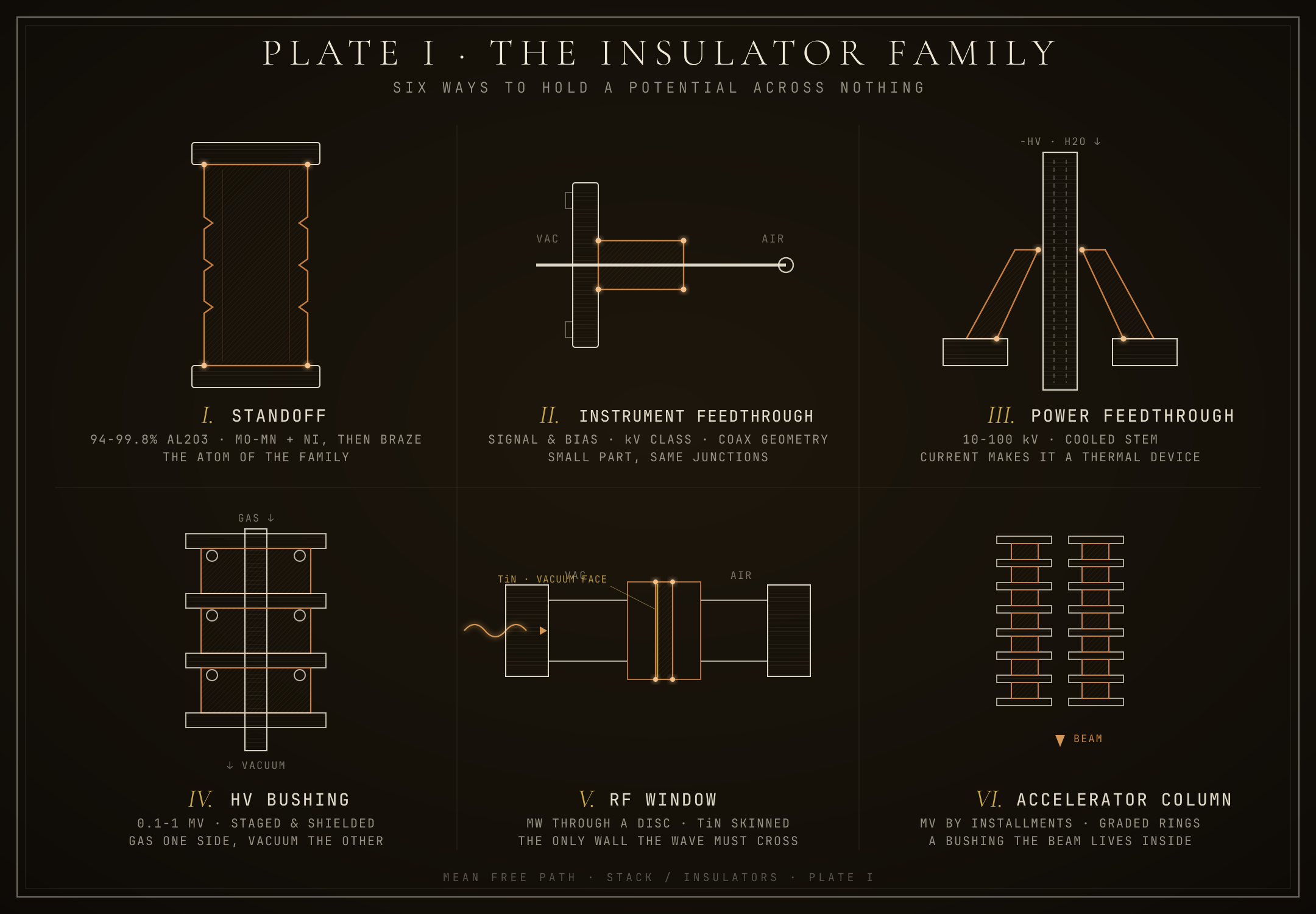
The standoff is the atom of the family: a cylinder that holds one electrode away from another and does nothing else. The instrument feedthrough carries signal and bias through the wall at kilovolt scale; small part, same junctions. The power feedthrough adds current, which adds heat, which makes it a thermal device with an electrostatic problem attached; the stem is often cooled and the ceramic sees a temperature gradient by design. The HV bushing is the aristocrat: staged ceramic rings, interleaved grading flanges, stress shields at every junction, gas on one side and vacuum on the other. The RF window holds no DC potential at all and still dies at the same address; megawatts cross a brazed disc whose surface must not multiply electrons. The accelerator column is a bushing the beam lives inside: potential by installments, ring by ring.
Materials follow a narrow canon. Alumina from 94 to 99.8 percent purity carries almost the entire family; purity buys lower dielectric loss and higher resistivity, and costs you metallization, because the classic Mo-Mn route bonds through the glassy phase that high purity removes. The 94 to 97.5 window is the metallization sweet spot; very high purity bodies and sapphire windows lean on active brazing instead, where a titanium-bearing alloy wets the ceramic directly. That titanium chemistry, and what it looks like inside the joint, is covered in Brazing and in the tomography essay Tight Enough. Aluminum nitride appears where heat must leave through the insulator itself. Whatever the body, the joint is the shared territory of this dossier and the brazing one: mechanically a seal, electrically a triple junction.
Ten decisions, one cross-section. Each rule states the move, the physics that pays for it, and the trap that comes with it.
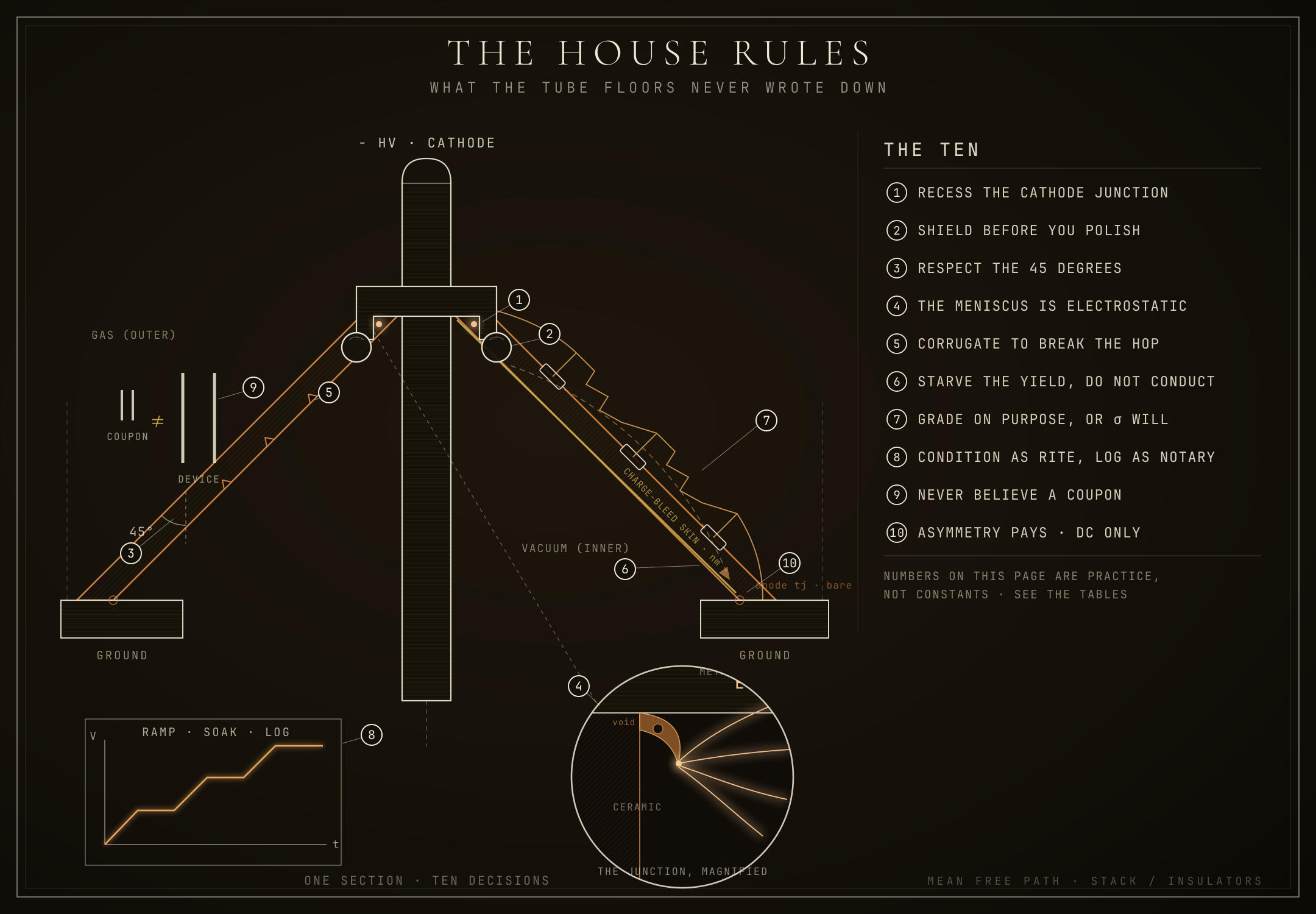
1. Recess the cathode junction. Pull the metal-ceramic-vacuum line into a shadowed groove where the macroscopic field is a fraction of the gap field. Physics: emission is exponential in local field; halving it buys orders of magnitude in current. Trap: the recess edge is itself a new geometry; give the lip its own radius or you have moved the problem, not solved it.
2. Shield before you polish. A toroidal screen overlapping the joint moves the high field from a brazed line you do not control onto a machined radius you do. Physics: the shield carries the equipotential crowding on polished metal, and the junction sits in its shadow. Trap: the shield-to-ceramic gap is a cavity; too tight and it hosts micro-discharges, facing up and it collects every particle you ever generate.
3. Respect the 45 degrees. Slope the insulator wall so electrons born at the cathode junction leave the surface instead of skating along it; the classic optimum sits near 45 degrees with the cone opening away from the cathode. Physics: the geometry starves the secondary avalanche of its runway. Trap: the trick requires knowing which electrode is the cathode; alternating stress makes the angle wrong half the time.
4. The meniscus is electrostatic. Specify the braze fillet as a field object: its radius, its wetting angle, its voids. Physics: a fillet that passes shear testing can still present a knife edge or a buried cavity, and each void is a private triple junction. Trap: braze volume control cuts both ways; starve the joint and you seed voids, flood it and the alloy runs onto the creep path and shortens it.
5. Corrugate to break the hop. Convolutions lengthen the surface path, but only if their depth and pitch interrupt the electron hop; decorative ripples add area, collect dust, and change nothing. Physics: the avalanche propagates by surface hops; a groove that swallows a hop resets it. Trap: corrugation roots concentrate mechanical stress, and brazing near them invites cracks.
6. Starve the yield, do not conduct. A nanometer-scale coating, titanium nitride or chromium oxide, drops the secondary electron yield below the multiplication threshold while staying thin enough to bleed charge without ohmic loss. Physics: no yield above unity, no avalanche; this is the whole defense of RF windows against multipactor. Trap: thickness is a cliff; too thick on a window absorbs power and delaminates, and coating the wrong face accomplishes nothing.
7. Grade on purpose, or sigma will. Divide the potential deliberately, with external resistor chains, semiconductive glaze, or interleaved electrodes. Physics: in steady DC the stress settles on whichever region is coldest and most resistive; heat remaps the stack whether you planned it or not. Trap: grading resistors dissipate and drift, and a divider that ages silently re-biases the one stage you cannot inspect.
8. Condition as rite, log as notary. Bring every new or vented insulator up in current-limited steps with soak plateaus; each micro-discharge burns off an emitter. Keep the record. Physics: conditioning is controlled destruction of the worst field emitters; the sequence, not just the endpoint, defines the state. Trap: condition with too much stored energy and you crater instead of polish; and a device separated from its logbook is a used machine with the odometer unplugged.
9. Never believe a coupon. Small-gap, small-area test data flatters you twice: breakdown field falls as gap grows, roughly as the square root at large gaps, and falls again as stressed area grows, because you are sampling for the worst defect. Physics: breakdown is extreme-value statistics; the biggest insulator finds the rarest flaw. Trap: multi-stage stacks do not share voltage equally, so the weakest ring sees more than its arithmetic share while your coupon saw less.
10. Asymmetry pays, DC only. With one fixed cathode there is one critical junction; spend everything there and leave the anode side plain. Physics: the anode junction initiates nothing as long as it stays the anode. Trap: every polarity transient, a grid breakdown, a switching event, briefly makes the safe junction cathodic; the MITICA bushing specification requires surviving reversal for exactly this reason.
The field lab puts the AC/DC argument under sliders. One bushing section, two field solutions computed offline and embedded in the page: the permittivity map and the conductivity map. A time slider blends between them with the real physics, one minus exp of minus t over tau, where tau follows epsilon times rho and rho follows an Arrhenius law with the temperature slider. A sine mode adds frequency and shows the crossover at f equals sigma over two pi epsilon. Readouts: field at the triple junction, tau, and crossover frequency, live. The teaching point falls out on its own: at room temperature the crossover sits at millihertz, so fifty hertz is deep in capacitive country, which is why the alternating century never needed to know sigma existed. Heat the ceramic toward three hundred degrees and the crossover climbs toward mains frequency, and the two countries begin to overlap. A model card on the page declares the equations, the first-order material model, and the validity limits; a lab that hides its model is a toy.
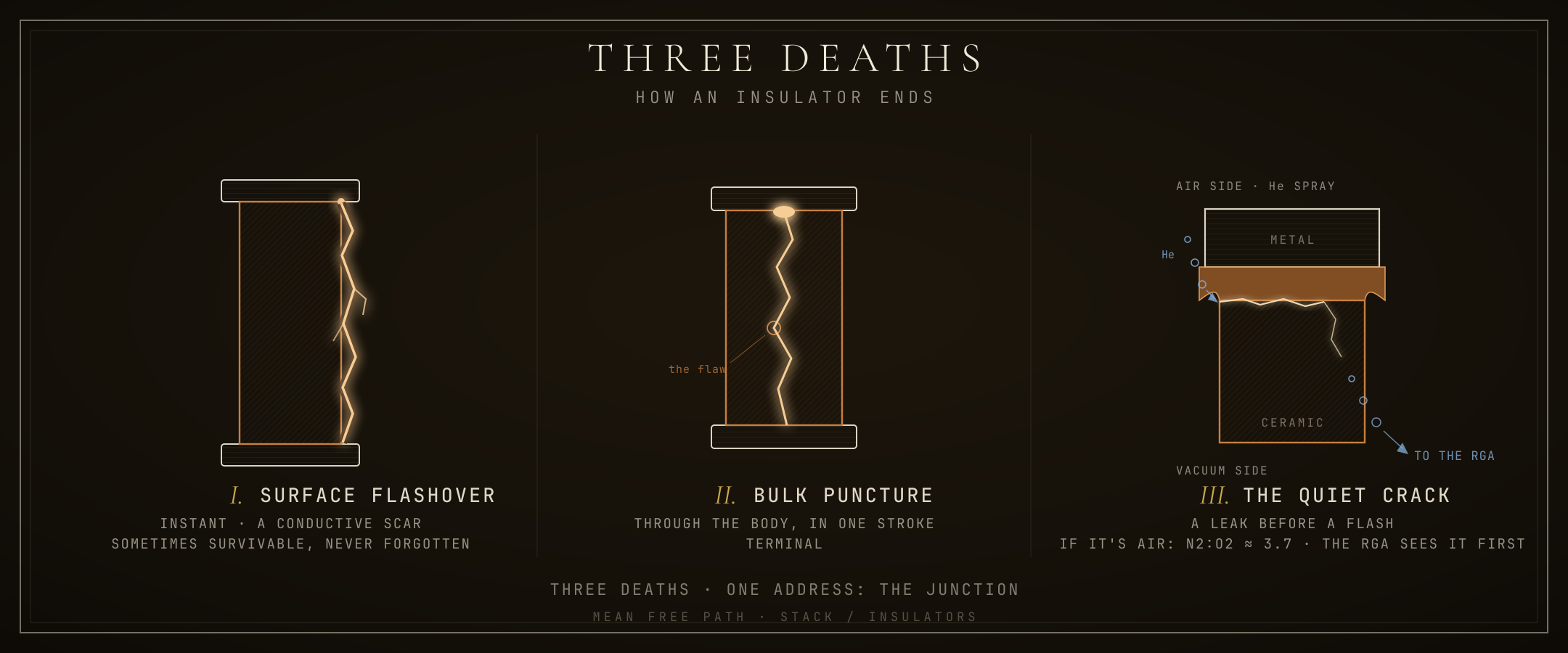
An insulator ends one of three ways. Surface flashover is the common death: sudden, bright, and sometimes survivable, but it leaves a conductive scar that lowers the next threshold; a part that has flashed is a different part. Bulk puncture is the rare death: a channel through the body, usually at a void or inclusion the coupon testing never sampled, and it is terminal. The braze crack is the quiet death: a joint that fatigues through thermal cycles and opens a leak long before it fails electrically. The residual gas analyzer sees this one first, and the signature is ordinary air, nitrogen to oxygen near 3.7, arriving steady and refusing to condition away. A flashover on an RGA trace is the opposite: a spike carrying the surface inventory, water, hydrogen, carbon monoxide, gone in seconds. Two failure modes, two time signatures, one instrument; this is where the insulator dossier hands off to fleet monitoring.
Practice values, not constants. They assume clean, conditioned, properly junction-engineered assemblies; derate hard for anything less.
Working stress, alumina in vacuum
| Stress | Design range | Note |
|---|---|---|
| DC, along surface | 3 to 8 kV/mm | conditioned, shielded junctions |
| AC crest, along surface | 0.5 to 0.7 x DC | use crest, never rms |
| Pulsed, microsecond class | 2 to 4 x DC | shorter is stronger |
| Bulk, through body | 10 to 20 kV/mm | mm-scale sections; surface fails first |
| Unshielded or unconditioned | derate 2 to 3 x | the junction tax |
Alumina, typical datasheet spread
| Grade | epsilon_r (1 MHz) | tan delta (1 MHz) | rho at 25 C | CTE, 25 to 300 C |
|---|---|---|---|---|
| 94 to 97.5% | 9.0 to 9.5 | 2 to 5 x 10^-4 | above 10^14 ohm cm | 6.9 to 7.3 ppm/K |
| 99.5 to 99.8% | 9.7 to 9.9 | about 1 x 10^-4 | above 10^14 ohm cm | 7.2 to 7.5 ppm/K |
The DC clock: tau = epsilon rho, alumina, epsilon_r near 9.8
| Temperature | rho, order of magnitude | tau | crossover f_c = 1/(2 pi tau) |
|---|---|---|---|
| 25 C | 10^14 to 10^16 ohm cm | 1.5 min to 2.4 h | 0.02 to 1.8 mHz |
| 150 C | 10^12 to 10^13 ohm cm | about 1 to 9 s | 0.02 to 0.2 Hz |
| 300 C | 10^10 to 10^11 ohm cm | about 10 to 90 ms | 2 to 18 Hz |
Mains frequency stays capacitive until the ceramic is seriously hot; direct current lives on the right-hand column from the first minute.
Interfaces
| Material | CTE, ppm/K | Role |
|---|---|---|
| Alumina 94 to 99.8% | 6.9 to 7.5 | the body |
| Kovar | 5.1 to 5.5 | the classic sleeve, to about 400 C |
| Ti-6Al-4V | 8.6 to 9.0 | active-braze partner, see Tight Enough |
| OFHC copper | about 17 | compliant thin sections only |
| AgCu eutectic braze | melts 780 C | the workhorse |
| AgCuTi active braze | about 800 to 850 C | direct-to-ceramic |
Paper to keep nearby: IEC 60270 for partial discharge measurement, IEC 60060 for high voltage test technique, IEC 60137 for bushings, ASTM D149 for dielectric breakdown of solids.
Who makes it
A short list of houses can metallize, braze, and test at the sizes and voltages this page describes, and the list gets shorter every year as the joint migrates from supplier catalogs into a few acquisition perimeters. The Actors World Map carries the current census, filtered on the insulator and ceramics sector; the essay on consolidation explains why the map looks the way it does. Two field notes survive any list: qualification of a new insulator house is measured in years, not purchase orders, and lead time on large brazed bodies is set by furnace queues you cannot see from a quote.
Sources · 15
- Cathode-junction emission, secondary-electron avalanche along the surface, gas desorption and flashover through the desorbed layer: the mechanism chain of The point and the surface-flashover death. Miller, H.C., Flashover of insulators in vacuum, IEEE Trans. Electrical Insulation 28, 512 (1993), and the twenty-year follow-up review
- Field-emission-driven initiation, conditioning as controlled destruction of the worst emitters, and the gap and area scaling behind house rule 9: Latham, R.V. (ed.), High Voltage Vacuum Insulation, Academic Press (The Physical Basis, 1981; Basic Concepts and Technological Practice, 1995)
- Local field an order of magnitude above the average at the metal-vacuum-dielectric line, and flashover initiation there: Li, High Voltage (2020)
- Enhancement set by the ratio of the angles the dielectric and the vacuum subtend at the corner, the physics under house rule 3: French & Pengvanich, J. Vac. Sci. Technol.
- Sloped insulator and the 45 degree optimum accelerators settled on, house rule 3: US Patent 9089039
- Screening the junction with a toroidal shield in pulsed high voltage, house rule 2: Phys. Rev. ST Accel. Beams
- Recessed junction and the extreme-value statistics of flashover, house rules 1 and 9: OSTI (2024)
- Titanium nitride on alumina drops the secondary electron yield to near unity above about 1 nm, and the coating should be as thin as possible: house rule 6 and the RF window of The Family. Michizono et al., Secondary electron emission of TiN-coated alumina ceramics, Vacuum
- The megavolt-class bushing as staged ceramic rings with interleaved grading flanges, and the polarity-reversal requirement that house rule 10 warns about: Final design of the HVD1 and Bushing for MITICA, Fusion Eng. Des.
- The 1.56 m ceramic ring and its Kovar braze, the largest insulator of this family actually built: JAEA / JSPF, Development of the High Voltage Bushing for the ITER NBI
- Moly-manganese metallization through the glassy phase, and why high purity costs joinability: the materials canon of The Family. Chiggiato et al., Manufacturing and Assembly for Vacuum Technology, arXiv:2006.12072
- Alumina datasheet spread of Numbers to Carry (epsilon_r, tan delta, rho at 25 C, CTE 25 to 300 C, for 94 to 97.5 % and 99.5 to 99.8 % grades). Rated [B], not [A]: the table is a spread read across supplier datasheets, and no single named datasheet is cited per row. To reach [A] it needs one named supplier document per grade band.
- Working-stress design ranges of Numbers to Carry (3 to 8 kV/mm DC along the surface, AC crest 0.5 to 0.7 x DC, pulsed 2 to 4 x DC, bulk 10 to 20 kV/mm, derate 2 to 3 x unshielded). Rated [B], not [A]: these are practice values carried by the tube houses, stated as such in the page. To reach [A] they need a published test series or a named standard behind each row.
- The DC clock table (tau = epsilon rho, crossover f_c) and the AC/DC field maps of The Lab are COMPUTED from the first-order material model the page declares in its own model card, not read from a source. Listed here so the reader knows which numbers on this page are measured and which are derived.
- Standards named in Numbers to Carry as papers to keep nearby: IEC 60270 (partial discharge measurement) and IEC 60060 (high-voltage test techniques) are verified; IEC 60137 (bushings) and ASTM D149 (dielectric breakdown of solids) are cited from trade usage and not verified against the published scope.
Rated [A] primary, [B] manufacturer or practice, [C] contextual. The physics of the triple junction and the three deaths rests entirely on primary sources; the working-stress and datasheet tables are practice values, rated [B] on purpose and flagged below for what they still need.