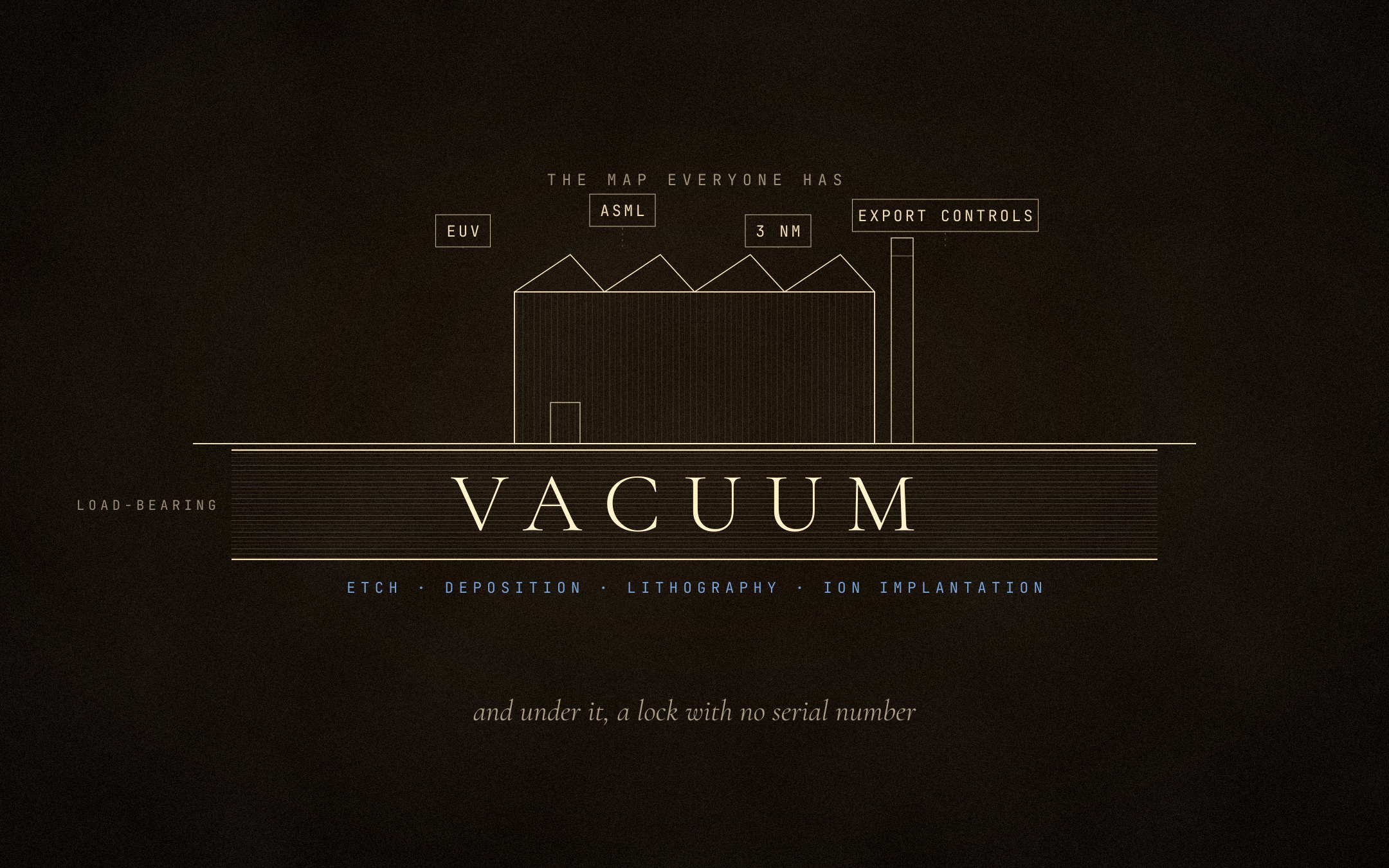
Everyone has a map of the chip war now.
The map has famous places on it. EUV. ASML. Taiwan. The 3-nanometer node. Export controls. The names are public, the stakes are public, the fight is on the front page. People who have never seen a wafer can tell you that one Dutch company makes the machine that prints the smallest chips, and that the United States is trying to keep that machine out of China.
That map is real. It is also incomplete. Under every place on it sits a layer that almost no one names.
That layer is vacuum, the engineering discipline: pumping a chamber down through more than ten orders of magnitude of pressure, holding it there and keeping it clean for years. Most of the critical wafer steps run inside pumped chambers, in near-emptiness.
The process is the vacuum
Walk the front end of a fab and count the steps that need a chamber pumped down. Almost all of them.
Deposition lays the thin films. Physical vapor deposition vaporizes a source inside a vacuum chamber and lets it condense on the wafer. Chemical vapor deposition feeds reactive gas at low pressure. Etching removes material with plasma, which only forms below atmospheric pressure. Ion implantation fires dopants down a vacuum beamline. Each layer of a modern chip is built and cut and doped this way, and a complex CMOS wafer runs the patterning cycle dozens of times before it is done.
- [B] HORIBA, semiconductor lithography process (a CMOS wafer can run the photolithographic cycle as many as 50 times), https://www.horiba.com/int/semiconductor/process/lithography/
Then there is the machine on everyone’s map. EUV. The light it uses is absorbed by ordinary matter, so the whole instrument has to live in vacuum. ASML says it plainly.
EUV light is absorbed by everything, even air. So the whole light path and everything the light interacts with, from source to wafer, must be in high vacuum.
- [A] ASML, EUV lithography systems, https://www.asml.com/en/products/euv-lithography-systems
Inside that source chamber, a high flow of hydrogen protects the collector mirror, and hydrogen is one of the hardest gases to pump. The pumps that do it are a product in their own right.
- [B] Pfeiffer Vacuum, vacuum solutions for EUV (high-flow dry pumps for hydrogen), https://www.pfeiffer-vacuum.com/global/en/markets/semiconductor/lithography/euv-lithography
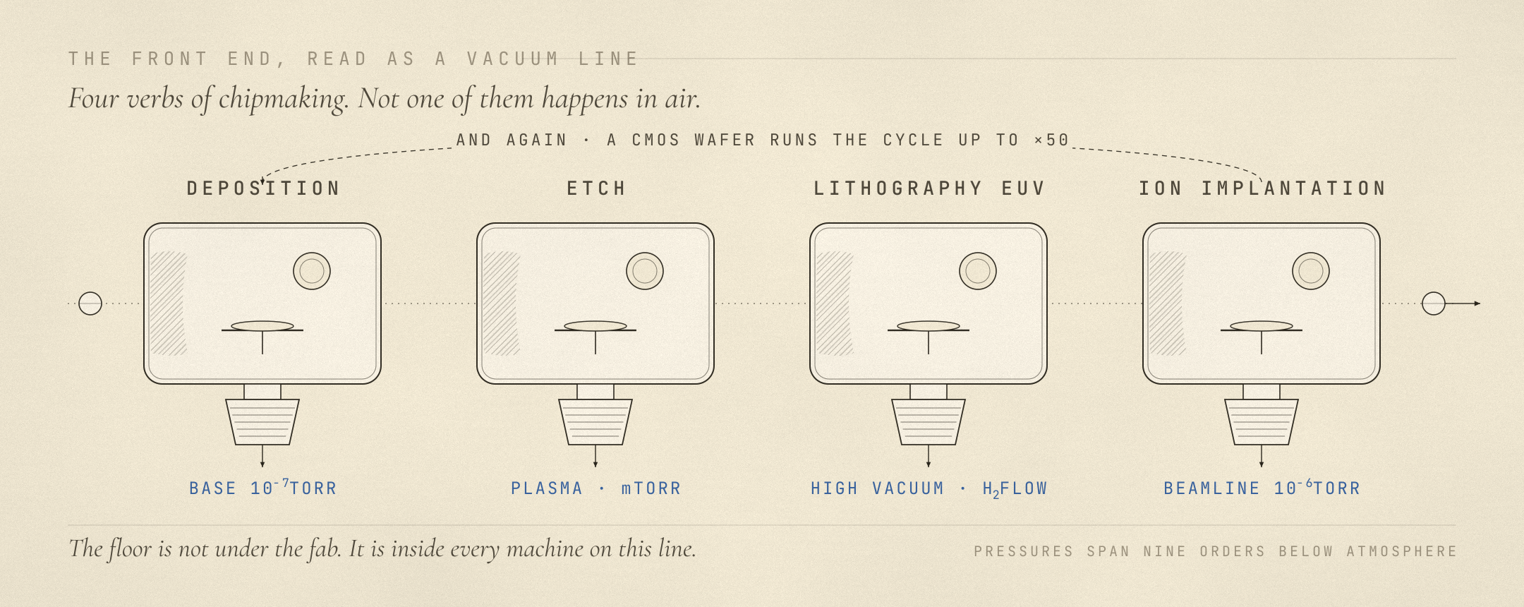
EUV therefore depends on vacuum as much as on light.
Who makes the pumps
Vacuum is the floor under the fab, and a short list of companies builds its pumps.
The market estimates disagree, and they disagree by a lot. One 2025 survey puts the top six pump makers at about 62 percent of the semiconductor vacuum pump market. Another puts a top five at 45 to 50 percent. A broader vacuum survey from 2023 puts a leading group at 25 to 30 percent. The three reports give three different shares, and all three are commercial, paywalled and silent on method.
- [C] Dataintelo, semiconductor vacuum pump market (top six ≈ 62%, 2025), https://dataintelo.com/report/semiconductor-vacuum-pump-market
- [C] Mordor Intelligence, vacuum pump market (top five ≈ 45–50%, 2025), https://www.mordorintelligence.com/industry-reports/vacuum-pump-market
- [C] GMInsights, vacuum pump market (leading group ≈ 25–30%, 2023), https://www.gminsights.com/industry-analysis/vacuum-pump-market
The same roster heads all three surveys.
Pull any of those rankings and the top of the list is that roster. Edwards, the dominant semiconductor vacuum brand, owned by Atlas Copco of Sweden, built in the UK. Pfeiffer, German, now inside Busch, German. Leybold, German. Ebara, Japanese. ULVAC, Japanese. Kashiyama, Osaka Vacuum, Canon Anelva, Japanese. The geography is the same in every survey.
The ownership is on the record, in the companies’ own filings.
- [A] Atlas Copco (Stockholm, Sweden), completion of the Edwards acquisition (Edwards headquartered in the UK), https://www.atlascopcogroup.com/en/media/press-releases/2014/140109-edwards
- [A] Pfeiffer Vacuum / Busch Group (Pfeiffer based in Asslar, Germany; Busch Group headquartered in Germany’s Black Forest; Busch holds a majority stake), https://group.pfeiffer-vacuum.com/en/news-media/press-releases/three-strong-brands-form-the-global-busch-group/
- [A] Ebara Corporation, corporate outline (headquartered in Tokyo, Japan; semiconductor vacuum pumps and abatement), https://www.ebara.co.jp/en/about/corporate/about/outline/index.html
The top tier is German, Japanese, British and Swedish.
That tier holds no American, Chinese or Russian maker. The Chinese names that do appear sit in the fragmented tail of every survey, the long list after the short one.
The United States, which runs the chip war, buys the floor its fabs stand on from allied makers. China, the country the chip war is aimed at, cannot make that floor either.
The control regime already knows
The export-control machinery has noticed, even if it never says the word.
When the United States moved to cut China off from advanced chipmaking, it wrote rules about tools. The October 2023 controls name the equipment by function. Etch. Deposition. Lithography. Ion implantation. Annealing. Metrology and inspection. Cleaning.
- [A] US Bureau of Industry and Security, Export Controls on Semiconductor Manufacturing Items, 88 Fed. Reg. 73424 (Oct. 25, 2023), https://www.federalregister.gov/documents/2023/10/25/2023-23049/export-controls-on-semiconductor-manufacturing-items
- [A] US BIS press release on the rule, https://www.bis.gov/press-release/commerce-strengthens-export-controls-restrict-chinas-capability-produce-advanced-semiconductors-military
Etch, deposition, advanced lithography and ion implantation are all vacuum processes. The control list is, in large part, a list of machines that cannot run without a pumped chamber. The state has drawn a fence around the vacuum frontier of the fab and labeled the fence by process.
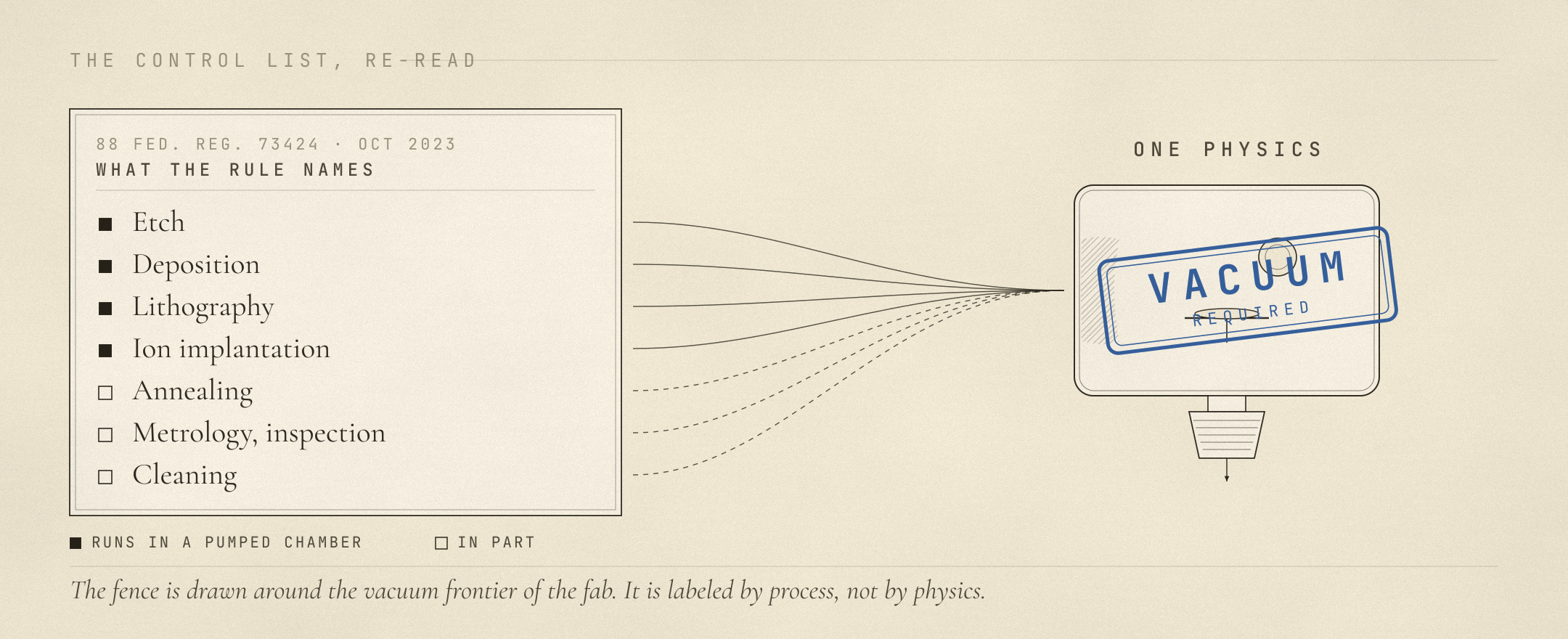
The export list therefore already protects the vacuum layer of the fab, under the names of the processes that depend on it.
What this movement does not settle
The evidence above covers what is visible. A pump has a serial number. A tool has a customs code. A factory has an address you can put under sanction. The lock described so far can be seen, counted and shipped, and a government can act on it.
A deeper lock sits under it.
You can buy a pump in a year and sanction one in a day. What cannot be done quickly is rebuild the forty years of hands that know how to balance a rotor, coat a surface and chase a leak no instrument has found yet. That tacit knowledge has no serial number and no line on the export list, so nobody counts it.

Movement II, The Names Nobody Cites, takes up what nobody counts. Underneath both sits the world map, one actor at a time.
Movement I of an open series on the geopolitics of vacuum. Sources are rated [A] standard or primary, [B] manufacturer, [C] secondary, the same scale used across The Stack. No internal lab data is used. This is open-source analysis of public material, offered for information only.
Sources · 2
- O'Hanlon, J.F., A User's Guide to Vacuum Technology, 3rd ed., Wiley, 2003.
- May, G.S. & Sze, S.M., Fundamentals of Semiconductor Fabrication, Wiley (load-lock and contamination-control chapters).
Ratings follow the Stack scale: [A] primary or standard, [B] manufacturer, [C] secondary. In-house derivations, anchors in O'Hanlon.